
Periodic and Metallic Nano-structures Patterned by Contact Transfer
Lithography with Application on Localized Surface Plasmon
Resonance
Hao-Yuan Chung, Chun-Ying Wu and Yung-Chun Lee
Department of Mechanical Engineering, National Cheng-Kung University, Tainan, Taiwan
Keywords: Localized Surface Plasma Resonance, Metallic Nano-structures, Contact Transfer Lithography.
Abstract: In this study, we demonstrate a rapidly, low cost, and mass production process to fabricate arrayed metallic
nanoparticles on a variety of substrates based on contact transfer and metal mask embedded lithography
(CMEL). A hexagonal arrayed metallic nanoparticles deployed on ITO/glass substrate with sub-micron
periodicity is achieved. It is observed in optical transmittance measurements that noble metallic arrayed
nanoparticles deployed on ITO/glass substrate result in a spectrally narrowband of extinction in visible
range, and is in good agreement with the simulated results using finite-element method (FEM). It is found
that the narrowband extinction spectrum is associated with electromagnetic field coupling between the
arrayed metallic nanostructures and the ITO layer. This electromagnetic field coupling induces significant
plasmon resonance in the ITO layer underneath the arrayed metallic nanostructures. Based on this observed
phenomenon and our innovative large-area nano-fabrication processes, optoelectronic devices with arrayed
metallic nanostructures can be easily designed and developed.
1 INTRODUCTION
Arrayed metallic nanoparticles have gained lots of
attentions in both scientific researches as well as
engineering application during last few decades.
Metallic nanostructures exhibit a rich variety of
intriguing optical properties due to the interaction of
the electromagnetic field with the free electrons of
the metal. Such an excitation can occur at a metal-
dielectric interface and is called surface-plasmon
polariton or at a metallic nanoparticle, and in this
case it is termed as particle-plasmon polariton
(Linden, Kuhl, and Giessen, 2001; Hutter and
Fendler, 2004; Yannopapas and Stefanou, 2004)
There are several ways to achieve metallic
nanoparticles, such as laser ablation method,
chemical reduction method and pyrolysis method
(Mafune et al., 2001; Pillai et al., 2007). These
methods can produce nanoparticles over large area
but have limitations to efficiently deploy
nanoparticles in specified arrangements. Electron
beam lithography is an excellent method to fabricate
arrayed metallic nanoparticles. The size of
nanoparticle can be well controlled to about several
tens of nanometers and arranged into square or
triangular lattice (Linden, Kuhl, and Giessen, 2001).
However, the costs of equipment and time-
consuming issues limit the capability to mass
produce large-area devices.
In this study, we demonstrate a rapidly, low cost,
and mass productive process to deploy arrayed
metallic nanoparticles on a variety of substrates
based on contact-transfer and mask-embedded
lithography (CMEL). A hexagonal arrayed metallic
nanoparticles deployed on an ITO/glass substrate
with sub-micron periodicity is obtained. Moreover,
the optical transmittance spectrum of the sample is
measured via spectrophotometer experimentally and
a numerical simulation using finite-element method
(FEM) is carried out to identify the mechanisms of
observed resonance characteristics.
2 EXPERIMENTAL DETAILS
AND RESULTS
This section describes the experimental details to
fabricate arrayed metallic nanoparticles on a variety
of substrates. A nanoimprinting process presented in
our previous study (Lee and Chiu, 2008), CMEL, is
applied to define and pattern arrayed metallic
structures which have feature sizes in sub-micron or
nanometer scales. First of all, a hexagonal arrayed
20
Chung H., Wu C. and Lee Y..
Periodic and Metallic Nano-structures Patterned by Contact Transfer Lithography with Application on Localized Surface Plasmon Resonance.
DOI: 10.5220/0005333500200025
In Proceedings of the 3rd International Conference on Photonics, Optics and Laser Technology (PHOTOPTICS-2015), pages 20-25
ISBN: 978-989-758-092-5
Copyright
c
2015 SCITEPRESS (Science and Technology Publications, Lda.)
structured silicon mold is prepared using electron
beam lithography. The diameter of each holed
structure is 200 nm and the periodicity of hexagonal
array is 400 nm. A flexible h-PDMS mold replicated
from the silicon mold is then obtained to act as the
imprinting mold used in CMEL process. This h-
PDMS mold is inexpensive compared to the primary
silicon mold thus could be disposable after being
contaminated or damaged during the imprinting
process. Furthermore, this flexible mold has benefit
to minimize the contact issue in imprinting process
and utilize large-area pattern transfer successfully.
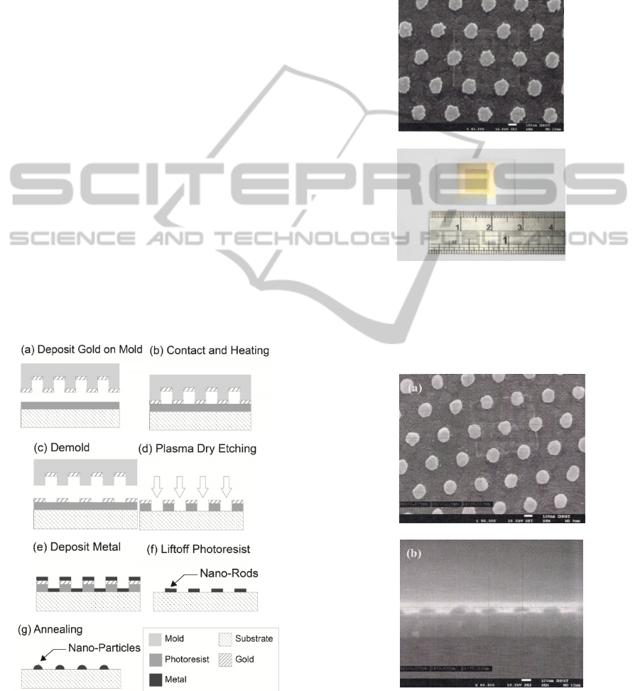
Figure 1 illustrates the procedures to fabricate
arrayed metallic nanostructures. An h-PDMS
concave mold deposited with gold film is contacted
to the top surface of polymer film coated on
substrate and then heating to the glass transition
temperature (Tg) of the polymer film. After cooling
down to room temperature, the patterned gold film is
transferred from the h-PDMS mold to the polymer
film owing to the good adhesion between metal-
polymer interfaces. This patterned gold film is then
acted as etching mask in dry etching process to
obtain a patterned polymer nanostructure.
Combining with lift-off and thermal annealing
processes, it is possible to fabricate arrayed metallic
nano-disks and nanoparticles on a variety of
substrates.
Figure 1: The procedure of using: (a-d) CMEL process, (e-
f) lift-off, and (g) thermal annealing processes, to achieve
an arrayed metallic nanoparticle.
Figure 2 shows the SEM image of the hexagonal
arrayed Au nano-disks (AuNRs) deployed on a 230
nm thick ITO film deposited on a soda-lime glass
substrate. The periodicity of hexagonal array is 400
nm; the dimensions of AuNRs are 200 nm in
diameter and 40 nm in thickness. The overall size of
arrayed metallic nanostructures is about 1 cm
2
.
(a)
(b)
Figure 2: (a) SEM images of the hexagonal arrayed
AuNRs deployed on 230 nm thick ITO film on top of a
glass substrate. The periodicity of hexagonal array is 400
nm; the dimensions of AuNRs are 200 nm in diameter and
40 nm in thickness. (b) The overall size of arrayed AuNRs
is about 1 cm
2
.
(a)
(b)
Figure 3: SEM images of (a) the top view and (b) the side
view of hexagonal arrayed AuNPs deployed on a 230 nm
thick ITO film on top of a glass substrate. Periodicity of
hexagonal array is 400 nm; the radius of AuNPs is 85 nm.
PeriodicandMetallicNano-structuresPatternedbyContactTransferLithographywithApplicationonLocalizedSurface
PlasmonResonance
21

Figure 3 shows the SEM images of the hexagonal
arrayed Au nanoparticles (AuNPs) deployed on an
ITO/glass substrate. During rapidly thermal
annealing process, the disk-liked AuNRs were
transformed into hemispherical AuNPs. The
periodicity of hexagonal array is 400 nm and the
radius of AuNPs is 85 nm. According to the
experimental results, arrayed metallic nanoparticles
deployed on ITO/glass substrates can be achieved.
The dimensions, shapes, and arrangements of these
arrayed metallic nanostructures can be easily
adjusted by using different type of imprinting molds.
The size and material combination of the obtained
metal particles can be controlled by the thicknesses
and varieties of metallic films deposited during the
lift-off process.
3 OPTICAL MEASUREMENTS
AND SIMULATIONS
The optical transmittance spectrum measurement of
these arrayed metallic nanoparticles is obtained
using a Hitachi U-3010 spectrophotometer. An
unpolarized light with wavelength λ
0
ranging from
400 nm to 1000 nm is normally incident onto the
metal side of these samples and the transmitted
power is collected at the substrate side. Figure 4
shows the transmittance spectrum of arrayed AuNRs
deployed on a glass substrate and on a 230 nm thick
ITO film coated on a glass substrate. It is observed
that the transmittance spectrum of both samples
exhibits a spectrally wideband extinction in near-IR
range due to localized surface plasmon resonance.
Moreover, significant narrowband extinction in
visible range is observed in case of arrayed AuNRs
deployed on ITO/glass which means a strong
electromagnetic field coupling between the arrayed
metallic nanostructures and the ITO layer.
Figure 4: The normal incidence transmittance spectrum
measurements of hexagonal arrayed Au nanorods on glass
substrate (dashed line) and on a 230 nm thick ITO film on
top of a glass substrate (solid line).
A numerical simulation using finite-element method
is carried out to identify the resonance phenomenon.
Both the transmittance spectrum and the
electromagnetic field distribution are obtained to
clarify the different mechanisms of resonances in
visible and near-IR spectrum. The dielectric
functions of Au and ITO are described as Drude
model (Rakic et al., 1998; Bender et al., 1998). The
dielectric constants of air and glass substrate are ε
air
= 1 and ε
glass
= 2.31, respectively.
Figure 5(a) and 5(b) demonstrate the
comparisons between the calculated transmittance
spectrums and experimental results of arrayed
AuNRs and AuNPs on a 230 nm thick ITO film on
top of a glass substrate. Figure 6(a) and 6(b) show
the simulated and experimental transmittance
spectrum of arrayed AgNRs and AgNPs on a 230
nm thick ITO film deposited on a glass substrate,
respectively. It is shown that the simulated results
are in good agreement with the experimental results.
The arrayed metallic nanoparticles deployed on
ITO/glass substrate result in a spectrally narrowband
extinction in visible and a wideband extinction in
near-IR both in experiments and in simulations.
0
20
40
60
80
100
400 500 600 700 800 900 1000
exp. simu.
Transmittance (%)
Wavelength (nm)
( a ) Au, Before Annealing
0
20
40
60
80
100
400 500 600 700 800 900 1000
exp. simu.
Transmittance (%)
Wavelength (nm)
( b ) Au, After Annealing
Figure 5: The normal incidence transmittance spectrum
measurements (solid line) and the simulated results
(dashed line) using FEM. (a) Before annealing, and (b)
after annealing.
Figure 7(a) and 7(b) reveal the simulated
electromagnetic field distribution of arrayed AuNRs
0
20
40
60
80
100
400 500 600 700 800 900 1000
AuNRs on glass
AuNRs on ITO/glass
Transmittance (%)
Wavelen
g
th
(
nm
)
PHOTOPTICS2015-InternationalConferenceonPhotonics,OpticsandLaserTechnology
22
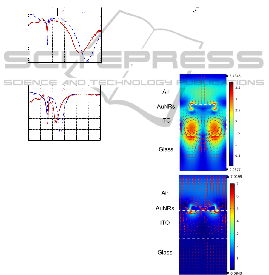
on a 230 nm thick ITO film deposited on a glass
substrate. While the incident wavelength λ
0
= 775
nm, as shown in Fig. 7, an enhanced electric field
around the metallic nano-disks due to localized
surface plasmon resonance is observed.
Furthermore, Fig. 8(a) and 8(b) show the significant
guided mode resonance in the ITO layer underneath
the arrayed metallic nanostructures when λ
0
= 556
nm.
0
20
40
60
80
100
400 500 600 700 800 900 1000
exp. simu.
Transmittance (%)
Wavelength (nm)
( a ) Ag, Before Annealing
0
20
40
60
80
100
400 500 600 700 800 900 1000
exp. simu.
Transmittance (%)
Wavelength (nm)
( b ) Ag, After Annealing
Figure 6: The normal incidence transmittance spectrum
measurements (solid line) and the simulated results
(dashed line) using FEM. (a) Before annealing, and (b)
after annealing.
Figure 7(a) and 7(b) reveal the simulated
electromagnetic field distribution of arrayed AuNRs
on a 230 nm thick ITO film deposited on a glass
substrate. While the incident wavelength λ
0
= 775
nm, as shown in Fig. 7, an enhanced electric field
around the metallic nano-disks due to localized
surface plasmon resonance is observed.
Furthermore, Fig. 8(a) and 8(b) show the significant
guided mode resonance in the ITO layer underneath
the arrayed metallic nanostructures when λ
0
= 556
nm.
A more detail discussion about the guided mode
resonance is started from a simple empty-lattice
approximation (Christ et al., 2004). As a first step of
this approximation, the energy dispersions of the
lowest transverse electric (TE0) and transverse
magnetic (TM0) guided modes of a homogeneous
ITO layer could be found from the solution of the
transcendent equations for the asymmetric
waveguide slab (Barnoski, 1973, pp. 53-72). It is
shown that the calculated dispersions of TE0 and
TM0 guided mode of a 230 nm thick ITO slab on
thetop of a soda-lime glass substrate. When
assuming a surface corrugation with periodicity d of
hexagonal array in a second step (in this case, d =
400 nm), the propagation constant is normalized to
the reciprocal lattice of the 2D photonic crystal slab
which equals to 4π/d
3
. While the propagation
constants of TE
0
and TM
0
equal to the reciprocal
lattice, it is shown that the photon energy of TE0
guided modes equal to 2.128 eV. These calculated
photon energy of TE
0
guided modes are in good
agreement with the simulated results using FEM.
The shifts of central wavelength might be caused by
the neglecting of material and geometry of metallic
deployed on the homogeneous ITO waveguide slab.
(a)
(b)
Figure 7: The electromagnetic field distribution of arrayed
AuNRs (before annealing) deployed on ITO layer; (a)
incident wavelength is 559 nm, and (b) incident
wavelength is 775 nm.
PeriodicandMetallicNano-structuresPatternedbyContactTransferLithographywithApplicationonLocalizedSurface
PlasmonResonance
23
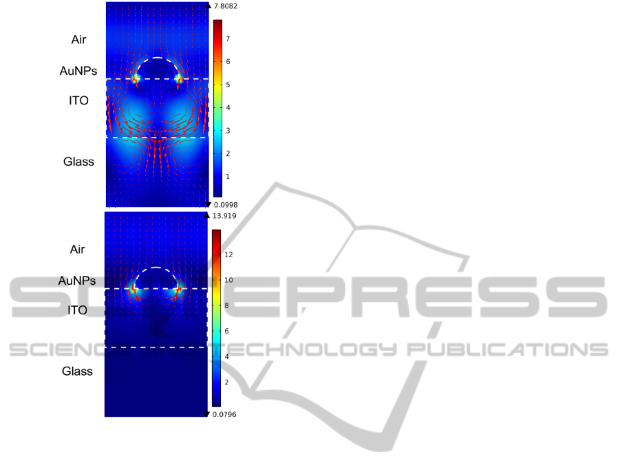
(a).
(b).
Figure 8: The electromagnetic field distribution of arrayed
AuNPs (after annealing) deployed on ITO layer; (a)
incident wavelength λ
0
= 556 nm, and (b) incident
wavelength λ
0
= 730 nm.
According to the FEM simulation and empty-
lattice approximation discussed above, it suggests
that the spectrally narrowband in visible range
owing to the guided mode resonance has quite
different resonance mechanism with respect to the
wideband extinction in near-IR range due to the
localized surface plasmon resonance. When an
electromagnetic wave normally incident onto
arrayed metallic nanostructures, a Bragg’s
diffraction phenomenon occurs and then couples the
electromagnetic wave into the waveguide slab. At
certain photon energies of the propagating guided
waves which the propagation constant equal to the
reciprocal lattice of arrayed nanostructures, a guided
mode resonance happens and enhanced electric field
distributes within waveguide slab can be observed.
4 CONCLUSIONS
In this study, we demonstrate a rapidly, low-cost,
large-area, and mass productive fabrication process
to obtain arrayed metallic nanostructures on a
variety of substrates. The key element in this
fabrication method is to combine an innovative
metal contact printing lithography with conventional
lifting-off and thermal annealing processes.
Hexagonal arrays of metallic nanoparticles with sub-
micron periodicity are successfully deployed on an
ITO/glass substrate. The dimensions, shapes, and
arrangements of these arrayed metallic
nanostructures and nanoparticles can be easily
adjusted by using different pattern designs in the
imprinting molds. The sizes and material
compositions of the obtained metal nanoparticles
can be easily controlled by the deposition
thicknesses and material varieties of films deposited
during the sample preparation process.
Optical transmittance measurements show that
certain kinds of noble metallic arrayed nanoparticles
deployed on an ITO/glass substrate can result in a
phenomenal narrowband of extinction in spectral
range of visible light. Theoretical analysis indicates
this narrowband extinction spectrum is associated
with electromagnetic field coupling between the
arrayed metallic nanostructures and the underlying
ITO layer. Numerical simulation based on finite
element method is carried out to demonstrate the
electromagnetic field distributions of the localized
surface plasmon resonance of arrayed metallic
nanostructures and the excited waveguide modes
within the ITO layer. This electromagnetic field
coupling induces significant plasmon resonance in
the ITO layer underneath the arrayed metallic
nanostructures. A further evidence is attained by
comparing the measured transmittance spectrum of a
similar noble metallic arrayed nanoparticles
deployed on a glass substrate. Experimental results
show that the narrowband extinction in visible
spectrum is vanished since there is no ITO layer to
support guided modes resonance. Based on this
observed phenomenon and our innovative large-area
nano-fabrication processes, optoelectronic devices
with arrayed metallic nanostructures can be easily
designed and implemented in the future.
REFERENCES
Bender, M., Seelig, W., Daube, C., Frankenberger, H.,
Ocker, B. & Stollenwerk, J. 1998 ‘Dependence of
oxygen flow on optical and electrical properties of
DC-magnetron sputtered ITO films’, Thin Solid Film,
vol. 326, pp.72-77.
Barnoski, M. K. 1973. Introduction to Integrated Optics,
Plenum Press, New York.
PHOTOPTICS2015-InternationalConferenceonPhotonics,OpticsandLaserTechnology
24

Christ, A., Zentgraf, T., Kuhl, J., Tikhodeev, S. G.,
Gippius, N. A. & Giessen, H. 2004 ‘Optical properties
of planar metallic photonic crystal structures:
Experiment and theory’, Phys. Rev B, vol. 70, p.
125113.
Hutter, E., Fendler, J. H. 2004 ‘Exploitation of localized
surface plasmon resonance’, Adv. Mater., vol. 16, pp.
1685-1706.
Lee, Y. C. & Chiu, C. Y. 2008 ‘Micro-/nano-lithography
based on the contact transfer of thin film and mask
embedded etching’, J. Micromech. Microeng., vol. 18,
p. 075013.
Linden, S., Kuhl, J., & Giessen H. 2001 ‘Controlling the
interaction between light and gold nanoparticles:
Selective suppression of extinction’, Phys. Rev. Lett.,
vol. 86, pp. 4688-4691.
Mafune, F., Kohno, J. Y., Takeda, Y., & Kondow, T. 2001
‘Dissociation and aggregation of gold nanoparticles
under laser irradiation’, J. Phys. Chem., vol. 105, pp.
9050-9056.
Pillai, S., Catchpole, K. R., Trupke, T. & Green, M. A.
2007 ‘Surface plasmon enhanced silicon solar cells’, J.
Appl. Phys., vol. 1019, p. 093105.
Rakic, A. D., Djurisic, A. B., Elazar, J. M. & Majewski,
M. L. 1998 ‘Optical properties of metallic films for
vertical-cavity optoelectronic devices’, Appl. Opt.,
vol. 37, pp. 5271-5283.
Yannopapas, V., Stefanou, N. 2004 ‘Optical excitation of
coupled waveguide-particle plasmon modes: A
theoretical analysis’, Phys. Rev. B, vol. 69, p. 012408.
PeriodicandMetallicNano-structuresPatternedbyContactTransferLithographywithApplicationonLocalizedSurface
PlasmonResonance
25
