
A FULLY INTEGRATED CMOS SENSOR FOR PICO-CURRENT
MEASUREMENT ON SOLID-STATE NANOPORE DEVICES
Jungsuk Kim
1
, Kenneth D. Pedrotti
1
and William B. Dunbar
2
1
Department of Electrical Engineering, University of California, Santa Cruz, CA 95064, U.S.A.
2
Department of Computer Engineering, University of California, Santa Cruz, CA 95064, U.S.A.
Keywords: Patch-clamp Technique, Solid-state Nanopore, Low-noise Biosensor, Single-molecule DNA Analysis.
Abstract: In this paper, an integrated high-sensitivity patch-clamp sensor is proposed to measure the ultra-low current
variation of a solid-state nanopore device. This sensor amplifier consists of three stages: 1) a headstage, 2) a
difference amplifier and 3) a unity-gain buffer. For the headstage, a resistive-feedback transimpedance
amplifier is employed to convert the small current to a readable voltage. The addition of a programmable
gain to the second-stage difference amplifier allows the maximum gain to be increased to 168dBΩ. This
sensor is fabricated in a 0.35μm CMOS process and is tested with an 80nm-diameter solid-state nanopore.
We present a detailed circuit analysis for the low-noise patch-clamp design and its noise measurement result
in this paper.
1 INTRODUCTION
For decades, the patch-clamp technique has been
utilized in electrophysiology and pharmacology to
analyze ion channels in living cell membranes and to
monitor the effect of drugs on their dynamics
(Hamill, 1981). Lately, this technique is also being
applied for single-moelcule DNA anlysis using both
biological nanopores and solid-state nanopores
(Branton, 2008). Figure 1 illustrates a conventional
patch-clamp sensor, comprised of a headstage and a
difference-amplifier stage, to monitor translocation
of individual DNA moledules through the nanopore
(Kim
1
, 2010). Here, the recording electrode (E
REC
)
follows the command voltage (V
CMD
) variation
applied to the non-inverting input of the differential
amplifier (A
1
) due to its high gain. This leads to an
electrical field between the cis and trans chambers
which are filled with a buffered ionic (KCl) solution.
Because the DNA backbone is negatively charged, it
can be captured into the pore, passing from the cis to
the trans chamber when a trans-side positive voltage
is applied. When the DNA traverses the nanopore,
the ionic currents carried by potassium (K+) and
chloride (Cl-) ions decrease in the range of tens to
hundreds of pAs. Figure 2 shows the cross sections
of a biological nanopore and a solid-state nanopore.
V
GND
V
CMD
R
F
DNA
cis
trans
E
REF
E
REC
I
IN
V
o
-
+
-
+
V
1
R
1
R
2
R
1
R
2
A1
A2
Nanopore
Figure 1: A conventional patch-clamp sensor to monitor
DNA translocation events through the nanopore.
DNA
Figure 2: Biological nanopore using α-haemolysin protein
(left) and soild-state nanopore using a silicon nitride layer
(right). Here, the biological pore dimensions were found
by crystallization (Song, 1996).
27
Kim J., Pedrotti K. and Dunbar W..
A FULLY INTEGRATED CMOS SENSOR FOR PICO-CURRENT MEASUREMENT ON SOLID-STATE NANOPORE DEVICES.
DOI: 10.5220/0003732000270031
In Proceedings of the International Conference on Biomedical Electronics and Devices (BIODEVICES-2012), pages 27-31
ISBN: 978-989-8425-91-1
Copyright
c
2012 SCITEPRESS (Science and Technology Publications, Lda.)

_
+
amp1
R
1
_
+
R
2
amp2
_
+
amp3
_
+
amp4
R
3
R
4
R
6
C
1
C
2
_
+
amp5
R
5
R
7
R
9
R
10
C
4
R
8
C
3
V
OUT
V
CMD
I
IN
V
CMD
Transimpedance
Amplifier (V/I)
Difference
Amplifier (V/V)
Unity gain
Buffer (
1)
I
IN
V
OUT
V
1
V
2
V
1
V
2
Figure 3: Proposed architecture of patch-clamp sensor.
To accurately monitor a DNA translocation event
througth the nanopore and convert its minute current
to a readable voltage range suitable for digitization,
a high-senstivity transimpednace amplifier (TIA) is
employed as the headstage of the patch-clamp sensor.
For design simplicity resistive-feedback (rf) TIAs
have been preferred to capacitive-feedback TIAs,
which require a periodic reset (Prakash, 1989). In
this work, we thus select an rf-TIA for the headstage.
Because the headstage makes a critical impact on
noise of the patch-clamp sensor, its noise analysis
and design parameters are consdiered in detail here,
with the goal of achieving an ultra-low input-
referred noise current. In addition to being low-noise,
the patch-clamp sensor requires a high enough gain
to amplify the small current signal. Use of a large
feedback resistor in the TIA can increase the gain at
the cost of chip area and bandwidth. Another way to
increase overall gain is to add a programmable gain
to the difference amplifier. More highly integrated
parallel patch-clamp arrays (Fertig, 2002) enable
multiple recordings as well as help save cost and
time. For such high-density patch-clamp sensors,
each sensing amplifier should dissipate low power.
In this work, we present the noise analysis and an
integrated circuit realization of a patch-clamp sensor
for solid-state nanopore applications. This sensor is
tested with the solid-state nanopore device that was
previously developed (Holmes, 2010).
2 SENSOR ARCHITECTURE
Figure 3 illustrates the proposed architecture of
patch-clamp sensor composed of three stages: 1)
headstage, 2) difference amplifier and 3) unity-gain
buffer. For the headstage an rf-TIA is realized using
an instrumentation amplifier topology that is capable
of minimizing the input-offset voltage (Kim, 2011).
For the difference amplifier, a resistive feedback
inverting amplifier having a gain of –R
4
/R
3
is chosen.
The observed DC variations in V
out
are used to
estimate nanopore conductance (S) (Healy, 2007).
Here the adjustable resistors R
4
and R
6
provide a
programmable gain, saving chip area by allowing
use of a smaller feedback resistor in the preceding
stage.
In order to drive pad, lead frame, pin, and probe
parasitics, a unity-gain buffer is selected for the
output stage. After the buffer an off-chip discrete
high-order low-pass filter (LPF) is used to further
restrict the patch-clamp sensor’s bandwidth. In this
work, a 5
th
-order Bessel LPF with a cutoff frequency
of 10KHz is adopted.
3 CIRCUIT IMPLEMENTATION
3.1 Noise Analysis
In nanopore sensing, the principal noise arises from
the nanopore device itself and the headstage. For the
noise analysis, their simplified electrical models are
illustrated in Figure 4. Here, R
N
and C
N
model the
resistance and capacitance of the nanopore device.
In the figure, R
E
models contact and probe resistance,
C
E
arises from the double layer capacitance of E
REC
.
R
E
is typically much smaller than R
N
.
In terms of this equivalent circuit of the nanopore
and E
REC
, the thermal noise current of the nanopore
and electrode is defined in Equation 1 (Kim
2
, 2010).
()
[]
fX
kT
fS
N
N
Re
4
)( =
(1)
()
=fX
N
()
(
)
()( ) ( )
EENNNENE
EENNENNE
RCRCfjRRCCf
CRRCRRfjRR
+⋅+⋅−
+
⋅
+
+
ππ
π
221
2
2
()
() ()
()
()
()
2
,
2
1
2
1
2
1,
2
1
1
2
1
1
1
1
1
1
Rn
P
AMPn
P
P
H
V
RsCsA
sA
R
V
RsCsA
RsCsAsA
R
fS ⋅
⎭
⎬
⎫
⎩
⎨
⎧
⋅++
⋅+⋅
⎭
⎬
⎫
⎩
⎨
⎧
⋅++
⋅⋅+
⋅≈
(2)
(3)
BIODEVICES 2012 - International Conference on Biomedical Electronics and Devices
28

2
,
1
Rn
V
2
1, AMPn
V
2
1,n
V
Figure 4: Simplified electrical model of nanopore, E
REC
and headstage.
Here, k and T are the Botzmann constant and
absolute temperature, respectively. The denominator
of Equation 1, X
N
(ƒ), denotes the impedance of the
equivalent circuit which is expressed in Equation 2.
Because DNA translocation events occur within a
bandwidth of 10KHz and R
E
is negligible compared
to R
N
, X
N
(ƒ) is approximately equal to R
N
at lower
frequencies. Therefore, S
N
(ƒ) is simplified to 4kT/R
N
which is proportional to the conductance of the
nanopore.
In addition to the noise current of the nanopore
and E
REC
, the input noise current of the headstage
has a critical impact on the background noise
because of its input-pair transistor’s 1/ƒ noise, which
increases at lower frequencies. In Figure 4, V
2
n,AMP1
and V
2
n,R1
represent the input-referred noise voltage
of the core-amplifier, amp1, and the thermal noise of
R
1.
The other stages’ noise sources are ignored
because of the relatively high gain of the headstage
(Kim
1
, 2010). Accordingly, the input-referred noise
current of the headstage at lower frequencies is
calculated in Equation 3.
The parameter C
P
is the parasitic capacitance
stemming from a coaxial cable, a BNC connector, a
copper line on PCB, a lead frame, a pad, an ESD cell
and input-pair transistors of the core-amplifier. A(s)
is the amplifier’s transfer function, A
0
/(1+s/ω
0
),
where A
0
and ω
0
represent its open-loop gain and
bandwidth. A(s) can be simplified to A
0
at lower
frequencies. Thus, 1/A(s) in Equation 3 is neglected,
leading to the simplified expression given by
() ( )
1
2
1,
2
4
2
R
kT
VCffS
AMPnPH
+⋅⋅≈
π
(4)
The second term in Equation 4 can be reduced by
increasing R
1
at the cost of larger area and a limited
bandwidth. To diminish the first term, V
2
n,AMP1
also
has to be as low as possible.
V
DD
V
SS
M
1
M
2
M
4
M
3
M
5
M
6
V
IN+
V
IN-
V
OUT
V
DD
V
SS
M
1
M
2
M
4
M
3
V
IN+
V
IN-
V
OUT
M
5
Figure 5: Self-biased differential Bazes amplifier (left) and
general differential amplifier (right).
According to Equations 1 and 4, the background
noise during the nanopore sensing is calculated as
() ( )
N
AMPnPB
R
kT
R
kT
VfCfS
44
2
1
2
1,
2
++⋅≈
π
(5)
This noise equation shows that the thermal noise of
the feedback resistor, 4kT/R
1
, is dominant compared
with the nanopore noise, 4kT/R
N
due to the usual
situation where R
N
>>R
1
. Thus to lessen the overall
background noise, a low-noise core-amplifier should
be designed for the headstage.
3.2 Low-noise Core-amplifier Design
A self-biased differential Bazes amplifier (Bazes,
1991), shown in Figure 5 (left), is used for the low-
noise core-amplifier design in this work. By virtue
of the symmetric structure of NMOS and PMOS
transistors, this amplifier is able to achieve both a
symmetrical positive and negative input common-
mode range (ICMR) and power-supply rejection
ratio (PSRR). Its structure also enables a high gain
because both the NMOS and PMOS contribute to
the effective transconductance (g
m
). Thus, its gain,
(g
m2
+g
m4
)×(r
o3
||r
o5
), where r
o
denotes the transistor
output resistance, is higher than the gain, g
m
×(r
op
||r
on
),
of a differential amplifier, as illustrated in Figure 5
(right), previously used (Weerakoon,2009). Dividing
the output equivalent noise by the squared gain of
the amplifier, the input-referred noise voltage of this
Bazes amplifier is approximately:
()()
()
noiseThermal
mm
noisef
ox
AMPn
gg
kT
fC
K
WLWL
V
2
42
/1
42
2
1,
8211
+
+⋅
⎥
⎦
⎤
⎢
⎣
⎡
+
=
γ
(6)
A FULLY INTEGRATED CMOS SENSOR FOR PICO-CURRENT MEASUREMENT ON SOLID-STATE NANOPORE
DEVICES
29
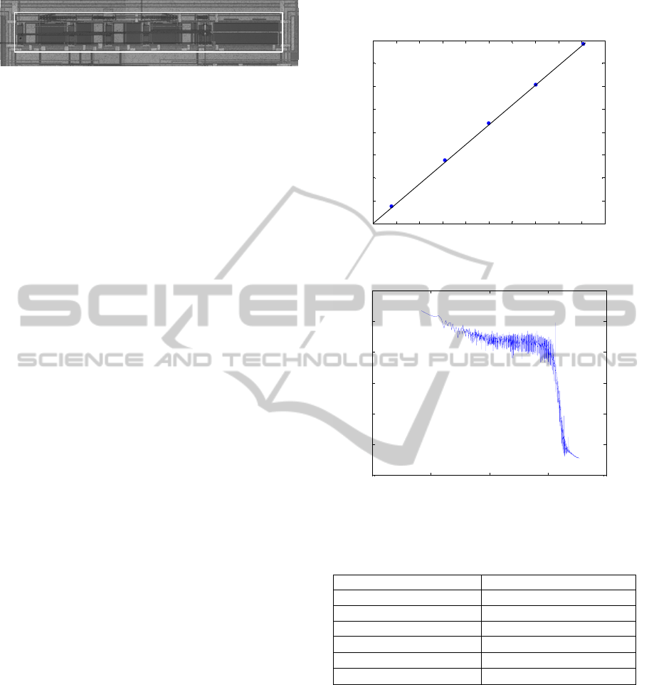
Figure 6: Chip micrograph occupying an active-die area of
980μm×121μm.
Here, K is a process-dependent constant on the order
of 10
-25
V
2
F. Because of the increased trans-
conductance of this topology, the thermal noise term
is smaller relative to a differential amplifier as well.
The 1/ƒ noise can be also reduced by enlarging
(WL)
2
and (WL)
4
. In this design, PMOS and NMOS
input pair transistors, with aspect ratios of 72μm/
1.5μm and 54μm/1.5μm, were used to reduce the 1/ƒ
noise.
4 TEST RESULTS
This patch-clamp sensor was fabricated in a 0.35μm
4M2P CMOS process and tested with an 80nm
diameter solid-state nanopore device. Figure 6
shows a micrograph of this prototype chip which
occupies an active-die area of 0.11858mm
2
.
The patch-clamp sensor has programmable gains
of 168, 161, 152 and 138dBΩ and accomplishes a
balanced ICMR of 1V
PP
which results from the
symmetrical structure of the core-amplifier. When
the gain is set to 168.2dBΩ, this amplifier consumes
a maximum power of 437μW.
Using the solid-state nanopore we measured an
open-channel current resulting from a DC variation
of V
CMD
across the nanopore conductance. Figure 7
displays the graph of the nanopore current verses
voltage whose slope yields its conductance. The
measured slope is 8.6nS and thus R
N
is 1/8.6nS ≈
116 MΩ.
Figure 8 shows the input noise spectral density of
the patch-clamp sensor. Due to the high-order LPF,
the noise dramatically decreases beyond 10 kHz.
The input root-mean-square (RMS) noise current of
this sensor is measured as 4.25pA at 10KHz
bandwidth, which is low enough to monitor DNA
translocation events that register tens of pA in
magnitude. The overall performance of the proposed
patch-clamp sensor is summarized in Table 1.
5 CONCLUSIONS
-550 -500 -450 -400 -350 -300 -250 -200 -150 -100 -50
-4.5
-4
-3.5
-3
-2.5
-2
-1.5
-1
-0.5
Command Volta
g
e
[
mV
]
Open Channel Current [nA]
Figure 7: Measured open-channel current variations.
10
-2
10
0
10
2
10
4
10
6
10
-24
10
-22
10
-20
10
-18
10
-16
10
-14
10
-12
Fre
q
uenc
y
[
Hz
]
Noise Spectral Density [A/sqrt(Hz)]
Figure 8: Measured input-noise spectra of the patch-clamp
sensor.
Table 1: Summary of chip performance.
DC gains 168, 161, 152, 138dBΩ
Input-referred noise 4.25pA
RMS
@168dBΩ
ICMR 1V
PP
Supply voltage ±1.5V
Max. power dissipation
437μW
Chip area 0.11858mm
2
Technology
0.35μm 4M2P CMOS
An integrated 4.25pA
RMS
-noise sensor has been
designed for pico-current measurements on a solid-
state nanopore device. To monitor the small current
variation through the nanopore, a resistive-feedback
transimpedance amplifier has been employed as a
headstage with a programmable gain added to the
second-state difference amplifier for additional gain.
This proposed sensor operates from ±1.5V, has four
different gains and consumes a maximum power of
437μW. This chip was fabricated in a 0.35μm 4M2P
CMOS process and tested. Using an 80nm-diameter
BIODEVICES 2012 - International Conference on Biomedical Electronics and Devices
30

solid-state nanopore, we measured the open-channel
current variations, resulting in a nanopore resistance
of 116 MΩ.
ACKNOWLEDGEMENTS
The authors are grateful to Prof. Holger Schmidt for
the solid-state nanopore fabrication funded by the
UCSC W.M. Keck Center for nanoscale optofluidics
as well as National Semiconductor Company for the
chip fabrication. This work is supported by US NSF
CAREER ECCS-0845766 (P.I: W.B. Dunbar).
REFERENCES
Hamill, O., et all, 1981. Improved patch-clamp techniques
for high-resolution current recording from cells and
cell-free membrane patches. European Journal of
Physiology, vol. 391, no. 2, pp. 85-100.
Branton, D., et all, 2008. The potential and challenges of
nanopore sequencing. Nature biotechnology, vol. 26,
no. 10, pp. 1146-1153.
Kim
1
, J., et all, 2010. An integrated patch-clamp amplifier
for ultra-low current measurement on solid-state
nanopore device. IEEE international SoC design
Conference, pp. 424-427.
Song, L., et all, 1996. Structure of staphy-lococcal α-
hemolysin, a heptameric transmembrane pore. Science,
vol. 274, pp. 1859-1866.
Prakash, J. Paulos, et all, 1989. A mono lithic patch-
clamping amplifier with capacitive feed- back. J. of
Neurosci. Methods, vol. 27, no. 2 pp. 165-172.
Fertig, N., et all, 2002. Nanostructured suspended aperture
for patch clamp recording and scanning probe
application on native membranes. Biophys. J., 78.
Holmes, M.R., et all, 2010. Micropore and nanopore
fabrication in hollow antiresonant reflecting optical
waveguides. J. Micro/Nanolith. MEMS MOEMS, vol.
9, no. 2, pp. 023004.
Kim, J., et all, 2011. On-chip patch-clamp sensor for solid-
state nanopore applicat- ions. Electronics Letters, vol.
47, no. 15, pp. 844-846.
Healy, D., et all, 2007. Solid-state nanopore technologies
for nanopore-based DNA analysis. Nanomedicine
(Lond), vol. 2, no.6, pp. 875-897.
Kim
2
, D., et all, 2010. Performance comparison of low
current measurement system for biomedical
applications. in Proc. of IEEE Int. Symp. Circ. And
Syst., pp. 3469-3472.
Bazes, M., 1991. Two novel fully complementary self-
biased CMOS differential amplifiers. IEEE J. of Solid-
State Circuit, vol. 26, no. 2, pp. 165-168.
Weerakoon, p., et all, 2009. An integrated patch-clamp
potentiostat with electrode compensation. IEEE Trans.
Biomed. Circ. And Syst., vol. 3, no. 2, pp. 117-125.
A FULLY INTEGRATED CMOS SENSOR FOR PICO-CURRENT MEASUREMENT ON SOLID-STATE NANOPORE
DEVICES
31
