
AN IMPROVED ON-CHIP DEBUG ARCHITECTURE
FOR SPARC PROCESSOR BASED ON SHADOW SCAN
TECHNIQUE
Liu Peng, Yu Lixin and Hui Qin
Beijing Microelectronics Technology Institute, Beijing, China
Keywords: On–Chip Debug, Shadow Scan, Embedded Processors.
Abstract: Because of the increasing design complexity of embedded microprocessors, pre–silicon verification in
design stage is insufficient to eliminate bugs (electrical and functional) and nonconforming chip behaviour
can still be found after the design is manufactured. Therefore, on–chip debug is becoming a key step both in
the implementation flow for the purpose of identifying and fixing design errors that have escaped pre–
silicon verification and in software development. In this paper, we present a new method of using improved
shadow scan architecture in the debug procedure which involves general–purpose registers in OpenSPARC
T2 processor and illustrate the mechanism of this logic and function module. The proposed architecture is
suitable for debugging work in practical embedded application, and provides more observability and
controllability which can reduce the time of scanning specified register window to 1/16 at the most.
1 INTRODUCTION
In pre–silicon verification stage of embedded
microprocessor development, design verification for
checking the correct circuit behaviour can be
performed mainly via simulation techniques using
testbenches and formal verification using different
levels of design abstraction. Due to simulation time
and limited resources, exhaustive simulation to
achieve 100% coverage with larger and complicated
designs becomes impractical.
Along with the bug escapes in the pre–silicon
stage, the inaccuracies in modeling integrated
circuits with process variation during the
manufacturing process are the main reason why
manufactured chips show operation misbehaviors or
fail to meet specifications. As for the software, the
development of software is becoming more and
more complicated and expensive. Debugging work
is a crucial stage in the development flow of
software nowadays.
Dramatic performance improvement of
microprocessor systems affects on–chip debugging
work in several ways: RISC based processors often
make use of instruction level parallelism to enhance
performance, which will lead to more complex CPU
micro–architecture and brings more difficulty to
access the internal processors states. Multi–core and
multi–thread technique also makes the access
inconvenient. But the urge of shorter development
time requires more internal CPU states observable
and controllable. Therefore, it is very important to
provide high performance and flexible debug
scheme to facilitate both hardware and software
development.
Traditional microprocessors use debug monitor
program to access target processor. This solution is
effective to some degree, but the drawbacks are also
obvious: the debug monitor program occupies
resources on the board, and it is intrusive to the
target system.
Another way of dealing with the debug problem
is through hardware assisted on chip. The solution is
implemented by inserting serial scan chains around
the datapaths to allow data to be scanned out through
JTAG interface. This approach makes debug
features such as hardware breakpoint, instruction
trace easy to implement. Therefore scan chains are
widely used to support manufacturing test, post–
silicon debug and software debug. However, it
requires halting the system to scan out responses
from the CUD (Circuits Under Debug). Hence, there
is a long time gap from the time when a bug is
invoked to when it is visible.
441
Peng L., Lixin Y. and Qin H..
AN IMPROVED ON-CHIP DEBUG ARCHITECTURE FOR SPARC PROCESSOR BASED ON SHADOW SCAN TECHNIQUE.
DOI: 10.5220/0003361504410444
In Proceedings of the 1st International Conference on Pervasive and Embedded Computing and Communication Systems (PECCS-2011), pages
441-444
ISBN: 978-989-8425-48-5
Copyright
c
2011 SCITEPRESS (Science and Technology Publications, Lda.)
Using shadow registers in the debug logic
circuitry can overcome the disadvantages of
debugging based on monitor program and the
inserting serial scan chain method. Shadow register
group is defined as a group of registers designed in
the microcontroller’s debug module, and the
registers will not intrude normal CPU operation.
They are often used to provide a non–destructive
scan out capability that preserves the existing system
state after the scan dump. Many systems are fully
scannable with non–destructive capability which is
helpful for both test and debug.
OpenSPARC T2 is a chip multi–threaded
processor which has eight SPARC cores, each
supporting concurrent execution of eight threads for
64 threads total. Integer Register File (IRF) is an
important part of the execution unit in SPARC core,
but can only be accessed by serial scan chains,
which makes the debug work ineffective. In this
paper, we will provide a solution to the limitation
mentioned above. In section II, we describe the logic
unit related to debugging work in OpenSPARC T2.
In section III, we illustrate the new on-chip debug
architecture based on shadow scan technique. The
logic architecture is applied in OpenSPARC T2
microprocessor. However, the methodology is
applicable to other processors.
2 OPENSPARC T2 LOGIC UNIT
RELATED
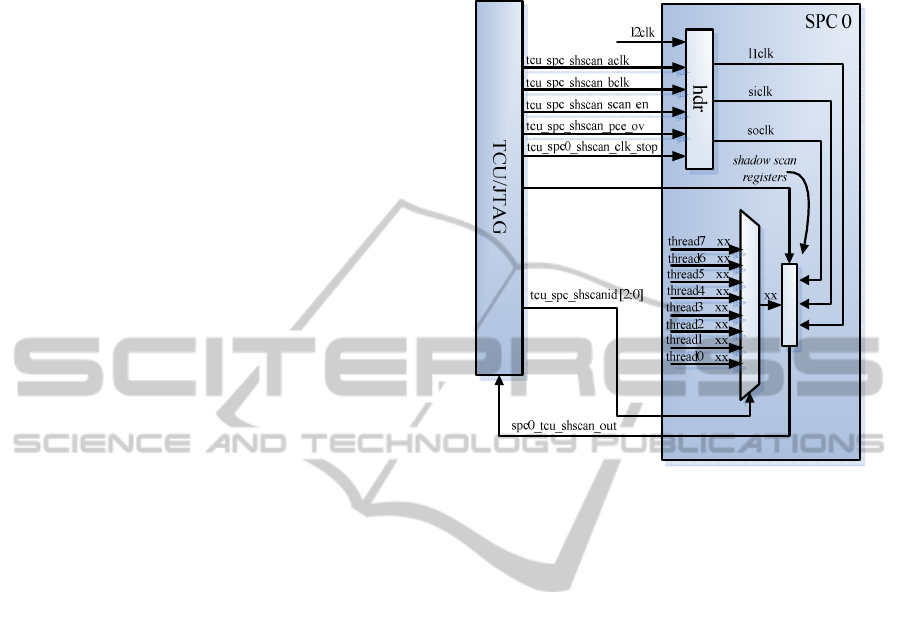
2.1 Shadow Scan Architecture
As stated in section I, scan chains are used to
support manufacturing testing and can be reused for
on–chip debug to increase debug capability. Scan
dumps give high observability of internal signals and
states after the occurrence of a triggering event.
However, they require halting the system to scan out
responses from the circuit–under–debug. This is
time consuming as many scan dumps may be
required. Shadow registers and shadow scan logic
are often used to provide a non–destructive scan out
capability that preserves the existing system state.
In OpenSPARC T2 microprocessor, each
physical SPARC core supports the ability to capture
a subset of each strand’s state for inspection via a
shadow scan facility. The architecture is shown in
Figure 1 (take SPARC core0 as an example). Each
core shadow scan will be contained in a separate
scan chain, with its own clock headers and controls
coming from the TCU (Test Control Unit, the main
test and debug support unit of OpenSPARC T2
Figure1: The Shadow Scan Architecture.
processor, which also controls the JTAG interface
and TAP machine of the processor). If a core is
disabled then its shadow scan contents will be
excluded and the number of TCK clocks should be
reduced to reflect the unavailable core(s).
The shadow scan function is controlled via JTAG
interface and invoked by JTAG commands. Eight
private JTAG instructions are defined to support
shadow scan operation of SPARC cores
(TAP_SPCTHR0_SHSCAN ~
TAP_SPCTHR7_SHSCAN). The high five ordered
bits of each instruction are the same, representing
the shadow scan operation. While the three low
ordered bits are different, and coded as strand ID,
illustrating the state of which thread of that SPARC
core needs to be captured.
The TCU continually specifies a strand ID to
each physical OpenSPARC T2 SPARC core. In
response, the physical core atomically captures the
state as described in Table I in a scan string. The
TCU then accesses the scan string and capture it in a
JTAG–visible register for presentation over the
JTAG interface.
2.2 Integer Register File
An UltraSPARC 2007 architecture specification,
processor should contain an array of general–
purpose registers. One set of 8 global registers is
PECCS 2011 - International Conference on Pervasive and Embedded Computing and Communication Systems
442
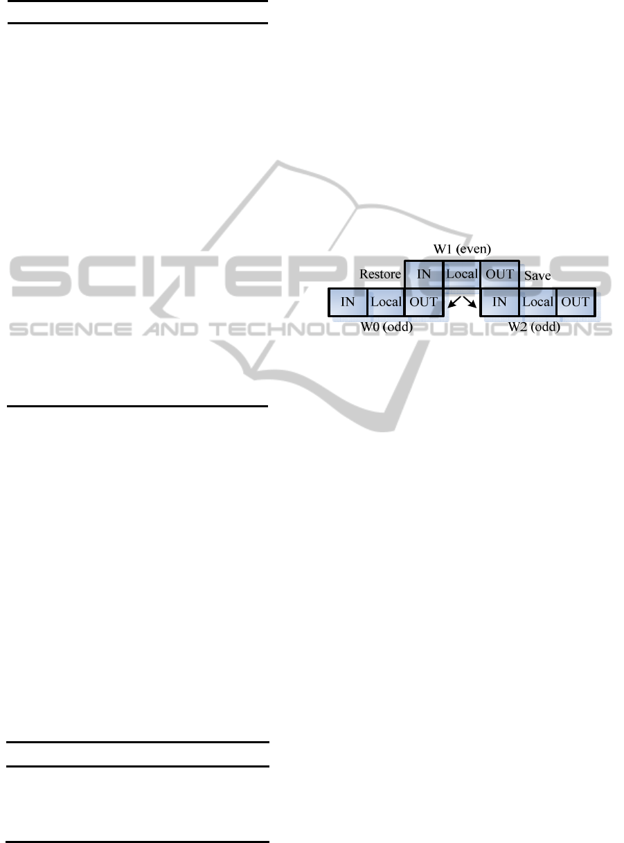
Table 1: SPARC Shadow Scan State.
Data Bits Field Remarks
117:72 VA [47:2]
Virtual address
Of last instruction
executed by that strand
71 ibe HPSTATE.ibe
70 cle PSTATE.cle
69 tle PSTATE.tle
68 tct PSTATE.tct
67 hpriv HPSTATE.hpriv
66 red HPSTATE.red
65 pef PSTATE.pef
64 am PSTATE.am
63 priv PSTATE.priv
62 ie PSTATE.ie
61 tlz HPSTATE.tlz
60:58 TL [2:0] TL
57:12 TPC [47:2] TPC for the last trap
11:3 TT [8:0] TT for the last trap
2:0 TL_FOR_TT [2:0] TL for the last trap
always visible. At any given time, a group of 24
registers, known as a register window, is also
visible.
A register window comprises the 16 registers
from the current 16–register group (referred to as 8
in registers and 8 local registers), plus half of the
registers from the next 16–register group (referred to
as 8 out registers). The names in, local, and out
originate from the fact that the out registers are
typically used to pass parameters from (out of) a
calling routine and that the called routine receives
those parameters as its in registers. The window
addressing is shown in Table II.
Integer register file (IRF) and register
management logic (RML) in the execution unit of
OpenSPARC T2 core are the hardware
implementation of general–purpose registers set
mentioned above.
Table 2: Windows Addressing.
Windowed Register Address R Register Address
in [0] – in [7] R [24] – R [31]
local [0] – local [7] R [16] – R [23]
out [0] – out [7] R [ 8 ] – R [15]
global[0] – global [7] R [ 0 ] – R [7]
RML is the logic control unit of IRF. The integer
register file is a 32–entry x 72–bit structure,
replicated four times for each thread. It has three
single ended read ports and two dual ended write
ports. The 32 entries are split into 16 I/O registers –
eight local registers and eight global registers. The
register file supports eight windows per thread. Each
local register is made up of eight basic registers, one
per window.
In addition, each thread contains one active
register, which has the contents of the current
window. Each I/O register has four basic registers,
which will be shared between even and odd
windows, and one active register for each thread.
The register file window structure is shown in
Figure 2.
Figure 2: The Register File Window Structure.
3 IMPROVED DEBUG
ARCHITECTURE
The original way to deal with the SPARC core
debug work, in which the IRF is involved, is using
serial scan chains in the IRF to allow data to be
scanned out through JTAG interface. That scan
chain is part of the long serial scan chain of SPARC
core and is not configurable, which means that in
order to obtain the internal and states, we need not
only to halting the system and stop the clock, which
may lead to the loss of data integrity, but also to wait
all the data on that chain to be dump out.
To overcome the disadvantages mentioned above,
the improvement we make can be summarized into
three aspects:
Adding new debug commands: Usually the
public or private JTAG instructions used in
debugging work are 8 bits long, but the new
instruction form (called TAP_SPCIRF_SHSCAN) is
twice the length of that. To decode these commands
correctly, we spilt them into two parts (8 bits each)
and change the decode module in TCU: When TCU
receives the high 8 ordered bits of
TAP_SPCIRF_SHSCAN instructions, it won’t
change the TAP machine to Capture–DR state to
capture date, but loop back to Capture–IR state
instead, waiting the whole instruction to be captured.
AN IMPROVED ON-CHIP DEBUG ARCHITECTURE FOR SPARC PROCESSOR BASED ON SHADOW SCAN
TECHNIQUE
443
The low five ordered bits of these instructions
determine which entry is read on port [2/1/0]
(because there are three reading ports under the
control of RML). Bits [4:1] are used to index into
one of sixteen wordlines. Decoding of 0 – 3
represents accessing to global registers, 4 – 7 odd
registers, 8 – 11 local registers, and 12–15 even
registers. Bit [0] is used for MUX 2 selection of 72
out of 144 columns. The two higher bits is read tid
and determine which thread is made available to the
read port. All ports see the same tid selection for
reads.
Reforming Shadow Scan Registers: The shadow
scan register in each SPARC core is a 118 bits
register which are split into two parts, working
separately to increase the efficiency. We widen this
registers and improve the control logic to make sure
the date captured from IRF is kept in independent
part of the register and – which is the most important
– can be shifted out from shscan_in port to
shscan_out port.
Figure 3: The Datapath of Improved Shadow Logic with
IRF.
Adding new datapaths: First we connect the
reading port of IRF with SSD module (the control
logic of shadow scan procedure in SPARC core) to
transfer the data to scan registers. In addition, we
add datapath among TCU, RML, IRF, and reuse
some RML logic module to make the read address,
tid specified in instructions and enable signals
known to IRF. The complete architecture of
adjunction, as shown in Figure 3, works as the
instructions direct and captures the information that
users need in IRF into shadow registers which are
visible over the JTAG interface.
4 CONCLUSIONS
In this paper, we have presented a method of using
improved shadow scan architecture in the on-chip
debug procedure in which IRF is involved. As we
can see from Table III, the new architecture provides
more controllability to processor users during
debugging work, at a cost of acceptable hardware
overhead. Moreover, the time that users spend on
debug is cut distinctly without halting the system.
The design has been verified on SPARC T2
processor and is found working well and efficiently.
Table 3: Comparison.
Original Improved
Clock Stop √ Χ
Time
Consuming
T T/16 (at
the best*)
Configurable Χ √
Extra Hardware
Overhead
Χ √
*: Without considering the time of decoding instruction
and state transition of TAP state machine.
REFERENCES
Chen Bilong, Yan Xiaolang, 2003. Method of Using
Shadow Registers in designing an on-chip Debug Unit
of a Microprocessor, Proc. Of International
Conference on ASIC.
Joon Sung Yang, 2009. Enhancing Silicon Debug
Techniques via DFD Hardware Insertion, phD thesis.
Xinli Gu, Weili Wang, Kevin Li, etc, 2002. Re-Using DFT
Logic for Functional and Silicon Debugging Test,
Proc. of International Test Conference.
Farideh Golshan, 2003. Test and On-line Debug
Capabilities of IEEE Std 1149.1 in UltraSPARC-III
Microprocessor, Proc. of International Test
Conference.
Sun Microsystems, 2007. OpenSPARCT2 Programmer’s
Reference Manual.
PECCS 2011 - International Conference on Pervasive and Embedded Computing and Communication Systems
444
